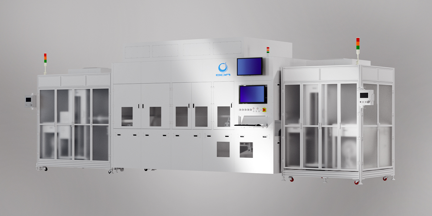
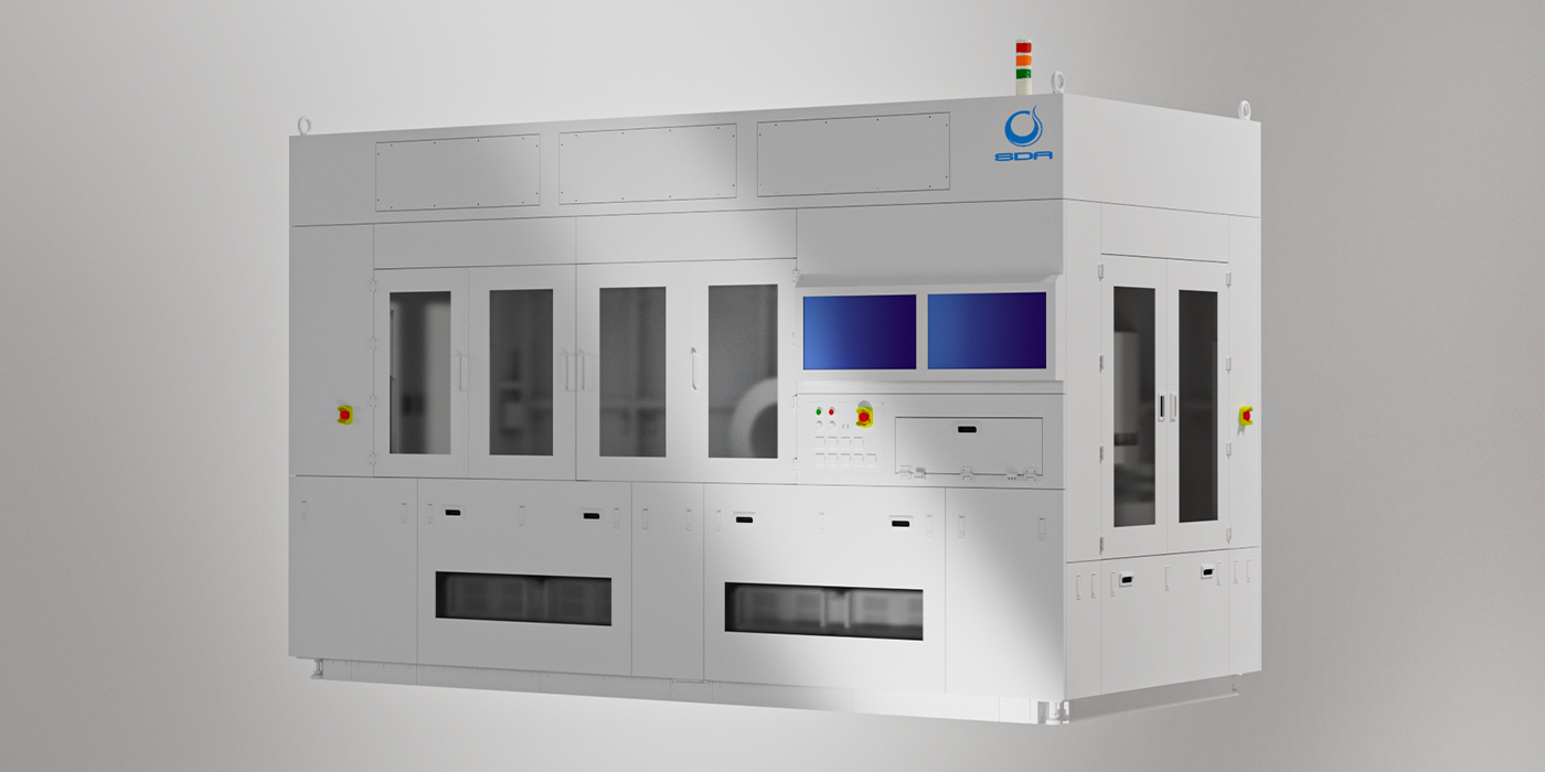
Direct Imaging System SDES Series
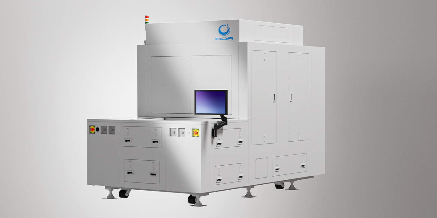
OUTLINE
- Process for all layer including inner, outer and Solder mask.
- Optimized for small quantities of many varieties.
- Prompt sample production lead-time
- Mass production for high density HDI
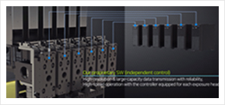
FEATURE
- High precision double-sided exposure technology.
- High intensity Light source
- Maximize productivity using Multi Optical Head
- Real time calibration technology for Scale and line-width
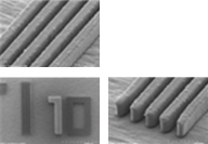
L/S=10um(DRF:25umt)
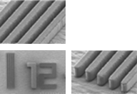
L/S=12um(DRF:25umt)
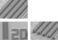
L/S=20um(DRF:25umt)
SPEC
| ITEM | SPEC | |
|---|---|---|
| Maximum imaging size | 650(W)x820(L)mm | |
| Data format | RS274X, GDSⅡ | |
| Light Source | Laser Diode | |
| Exposure Wavelength | 405nm | |
| Minimum Pattern size | 20um L/S | |
| Data Resolution | 1um | |
| Overlay | ≤±10um | |
| Throughput | 20sec (@20mj) | |
| Auto-Scaling | Yes | |
| Auto-Calibration | Yes | |
| Calibration of partial | Yes | |
| Panel Tracking | Yes | |
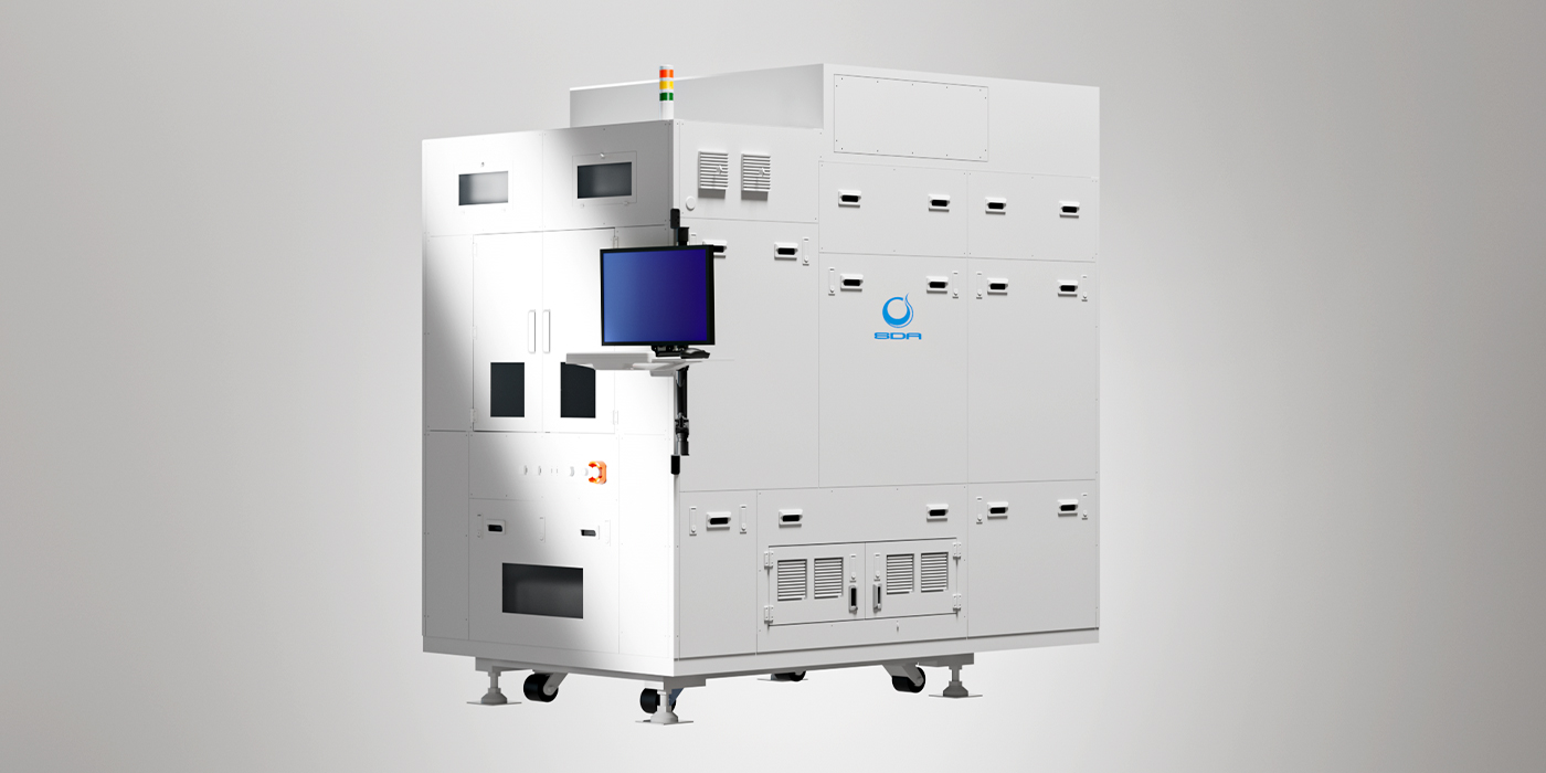
Direct Imaging System Roll to Roll
OUTLINE
- Roll to Roll Automatic equipment
- Sheet Type Manual production
- Support for smart factory system integration
- Prompt sample manufacturing lead-time
- Mass production for High density of HDI
FEATURE
- High precision double sided exposure
- High intensity laser sources
- Maximize productivity with Multi optical head.
- Real time calibration of scale and line-width
- High precision Overlay
L/S=10um(DRF:25umt)
L/S=12um(DRF:25umt)
L/S=20um(DRF:25umt)
SPEC
| ITEM | SPEC | |
|---|---|---|
| Maximum imaging size | 2000(W)x520(L)mm | |
| Data format | RS274X, GDSⅡ | |
| Light Source | Laser Diode | |
| Exposure Wavelength | 375nm, 405nm | |
| Minimum Pattern size | 20um L/S | |
| Data Resolution | 1um | |
| Overlay | ≤±9um | |
| Throughput | 25sec (@23mj) | |
| Auto-Scaling | Yes | |
| Auto-Calibration | Yes | |
| Calibration of partial | Yes | |
| Panel Tracking | Yes | |
Direct Imaging System META Series
OUTLINE
- High resolution exposure system for semiconductor package field.
- Top notched L/S 5um line-width formation
- LDI Equipment optimized for Semiconductor package/Wafer MEMS 4~12”
- L/S 2/2um, 5/5um for high density and scaling-down package technology
FEATURE
- High resolution scaling-down line width
- High intensity laser (375,405nm)
- Maximize productivity using Multi Optical Head
- High precision Overlay
Independent exposure head configuration
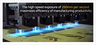
High speed exposure
SPEC
| ITEM | SPEC | |
|---|---|---|
| Maximum imaging size | 650(W) x 900(L) mm, 2100(W) x 620 (L)mm | |
| Data format | RS274X, GDS, ODB++ | |
| Light Source | Laser Diode | |
| Exposure Wavelength | 375nm, 405nm | |
| Minimum Pattern size | 2um L/S | 5um L/S |
| Data Resolution | 0.1um | 0.25um |
| Overlay | ≤±1um | |
| Throughput | 39sec (@20mj) | |
| Auto-Scaling | Yes | |
| Auto-Calibration | Yes | |
| Calibration of partial | Yes | |
| Panel Tracking | Yes | |
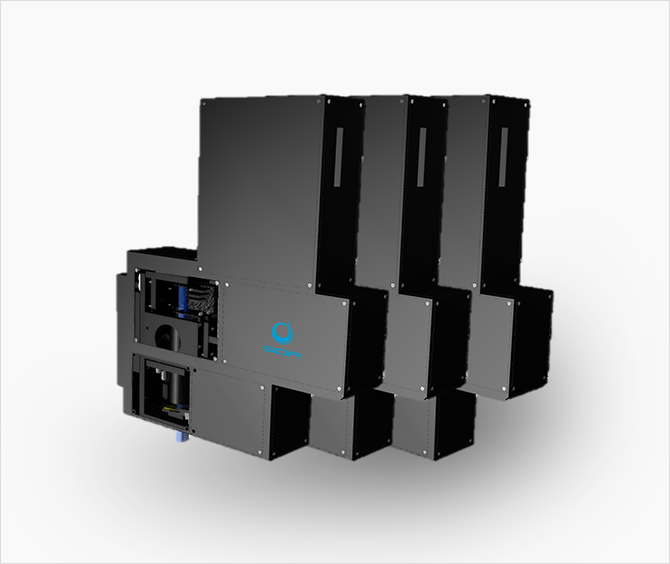
Direct Imaging System SDES-LDI2000 Series
OUTLINE
- High efficiency, High productivity L/S 10um/20um exposure engine
- 2 wave length light source (365nm, 405nm)
- Applicable to High aspect ratio substrate(Basic 600x2,000)
- Capable of arrangement at one time (Maximum 600x2,000 1EA or 300x2,000 2EA)
- Capable of Batch exposures through multi Substrate arrangement
- Capable of Multi layout alignment Scale calibration
- Divided-Calibration inside of substrate is possible
- By split exposure, Maximum 4m substrate divided exposure is possible
FEATURE
- High efficiency, High productivity exposure head
- High intensity light source (375nm, 405nm)
- Maximize productivity using Multi Optical Head
- Batch exposures through Multi Substrate arrangement
- Implementation of Divide Exposure Function
SPEC
| ITEM | SPEC | |
|---|---|---|
| Maximum panel size | 650(W)x2,050(L)mm 0.2~2mm thickness | |
| Maximum imaging size | 600(W)x2,000(L)mm | |
| Data format | Gerber data(RS274X) ODB++ (Option) | |
| Light Source | Laser Diode Module (5W, 12W, 30W) | |
| Exposure Wavelength | 405nm : 5W, 10W, 30W 375nm : 10W *Total : 40W | |
| Minimum Pattern size | 20um L/S | |
| Data Resolution | 1um | |
| Overlay | ≤±9um | |
| Tact time | < 120sec (@200mj, 175mmx2,000mm) | |
| Auto-Scaling | Yes | |
| Split Calibration | Yes | |
| Divided align | Yes | |
| Panel Tracking | Yes | |
Lithography System SDLM-Optics
OUTLINE
- Optical system for manufacturing DI(direct Imaging) Exposure equipment and data transmission module
FEATURES
- L/S(Line & Space) : 5, 10, 20um
- Light source : Laser diode 375, 405 wave length. (Singular wave length is possible)
- PCB, Wafer, Package Substrate, MEMS and Mask Writer, etc.
- Can be applicable to exposure fields.
- Development platform in Windows settings provided.
- Trigger-Based Synchronization functionality provided
High-Performance Modules for Direct Imaging
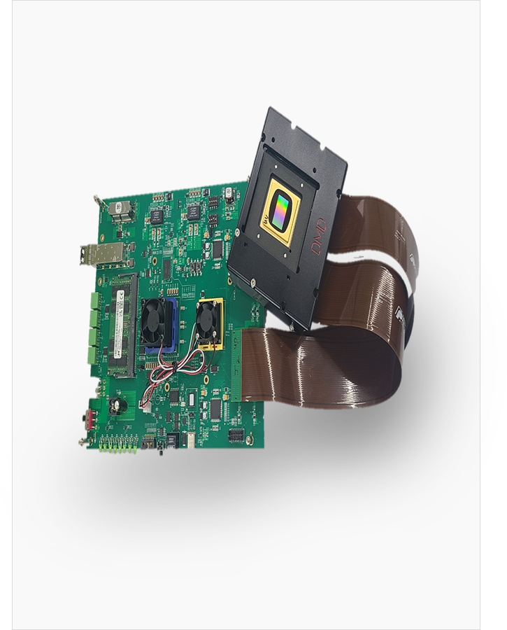
OUTLINE
- Application in the manufacturing of DMD (TI, USA) based equipment
such as DI (Direct Imaging) machines, 3D scanners, and 3D printers. - Development platform
· OS : Windows 10 or higher version
· Tool : C#, Visual C++
· Format : SDK
SPEC
| ITEM | SPEC |
|---|---|
| Chipset | DLP9500 & DLPC410 |
| DLP Format | 0.95” 1080p |
| Window Options | VIS, UV |
| Micromirrors | 1920 x 1080 |
| Data Format | Gerber(RS274x) |
| Speed | ~22,000fps(Frame Per Second) |
| Data Resolution | 0.05~2um |
| PC Interface | 10G Ethernet |
